
FULL-WAVE RECTIFIERS AND POWER SUPPLIES
PURPOSE:
The experiment is to study the performance and characteristic of full-wave rectifiers and DC power supplies utilizing Zener diode as a voltage stabilizing device. The performance of the full-wave rectifier will be studied and measured as well as that of the Zener diode.
INTRODUCTION:
One of the important applications of the P-N junction diodes is in converting alternating current (AC) into direct current (DC). Half-wave rectifiers can be used, but they are highly inefficient in converting AC power to DC power. Additionally, they have high contents of harmonics, which are difficult to filter out and to smooth out the ripple in the rectified AC power. On the other hand, full-wave rectifier improves on the conversion efficiency of AC power to DC power
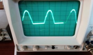 Fig .1. System generated DC waveform
It will also reduce the harmonic contents of the rectified waveform and reduce the requirement on the smoothing filter needed to reduce the ripple in the rectified waveform. A typical waveform of a full-wave rectifier is shown in Fig. 1.
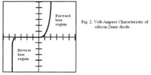 Fig. 2. Full-wave rectifier output waveforms. The dark line is the filtered output, while the thinner line is the unfiltered output.
Zener diodes are special diodes designed to maintain fixed voltages across the load. They are designed to “breakdown” in a reliable and non-destructive way when they are biased in the reverse direction by a voltage higher than the breakdown voltage. A typical DC characteristic of the Zener diode is as shown in Fig. 2. The knee in the reverse bias region in Fig. 2 is the “break down voltage” of the Zener diode. However, this voltage is also known as the Zener voltage.
Zener diodes are rated by their breakdown voltage and maximum power. The minimum Zener voltage available is 2.7 V while power ratings of 400 mW and 1.3 W are common. The connection diagram of the Zener diode as a basic voltage regulation circuit is as shown in Fig. 3.
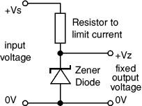 Fig. 3. The connection of the Zener diode as a voltage regulator.
A complete and stabilized power supply can be obtained by using the rectifier diodes to change the AC power to DC power. The rectified voltage is filtered to reduce the ripple on the rectified waveform. A Zener diode is then used to regulate the voltage to its desired final value. A simple breadboard diagram of a power supply is as shown in Fig. 4.
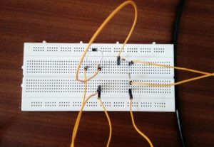 Fig. 4. Breadboard diagram of the rectifier.
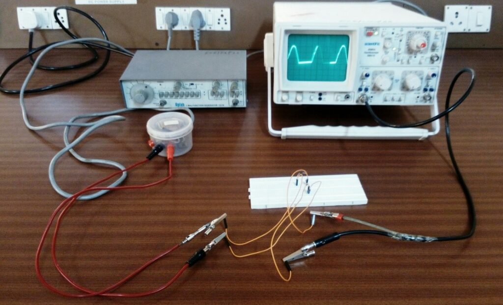
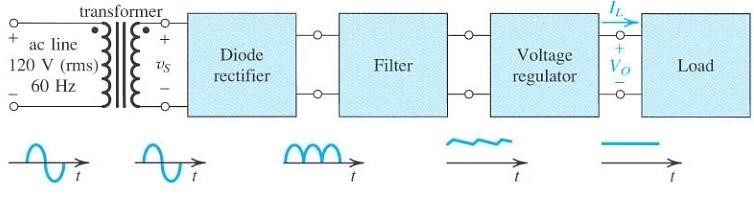 Fig. 5. A simple block diagram of regulated DC power supply.
In this block diagram, each individual block is described in more detail below:
- Transformer: steps down high voltage AC mains to low voltage AC.
- Diode rectifier: converts AC to DC, but the DC output has large ripple component.
- Filter: smooth the DC from varying greatly and reduces the ripple component.
- Voltage regulator eliminates ripple by setting DC output to a fixed voltage.
- The load is the part of the circuit to which the DC power is delivered to perform the useful operation.
LAB WORK:
- Measurement of the DC characteristic of the Zener diode
1.1 Set the DC voltage of the power supply to 0V.
1.2 Connect the Zener diode circuit as shown in Fig. 5.
1.3 Change the DC supply voltage in small steps. Use a digital voltmeter, measure Vin, VR, and VD as defined in Fig. 5. Tabulate your measurement data.
1.4 For each step, calculate the DC current through the diode, which is equal to (VR / 2000).
1.5 Reverse the polarity of the DC power supply in Fig. 5. Repeat the measurement steps from 1.1 to 1.4.
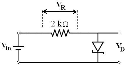 Fig. 5- Connection diagram for measuring the DC characteristic of the Zener diode.
- Characteristic of the bridge rectifier.
2.1 Connect the full-wave rectifier circuit as shown in Fig. 6 in which RL = 1 kW.
Do not connect any capacitor across the load.
2.2 Monitor Vo (see Fig. 6) on the oscilloscope. DO NOT monitor Vs and Vo on the oscilloscope simultaneously. Measure the peak input and peak output voltages. Capture the displayed waveform. Use a digital voltmeter, measure the DC voltage across RL.
2.3 Connect 47 mF across RL. Monitor Vo on the oscilloscope and capture the waveform. Repeat the measurement with 10 mF capacitor.
Compare the two rectified waveforms obtained with the different capacitors.
2.4 Change the load resistor to 10 kW and 100 kW and monitor the rectified voltage at the output. Comment on the impact of the load resistance on the output ripple.
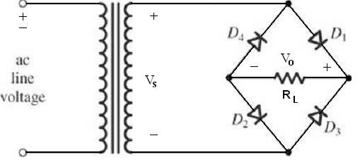 Fig. 6. Unfiltered full-wave rectifier using bridge connection of the diodes.
- Characteristic of the center-tapped full-wave rectifier
3.1 Perform the necessary measurement on the center tapped transformer to determine which lead is the center tap.
3.2 Connect the full-wave rectifier circuit as shown in Fig. 7 in which RL = 1 kW. Do not connect any capacitor across the load.
 Fig. 7. Unfiltered full-wave rectifier circuit used in the experiment.
3.3 Monitor both Vs and Vo (see Fig. 7) on the oscilloscope simultaneously. Measure the peak input and peak output voltages. Sketch the displayed waveforms. Use a digital voltmeter, measure the DC voltage across RL.
3.4 Connect 47 mF across RL. Monitor Vs and Vo on the oscilloscope and capture both waveforms.
- Regulated DC power supply
4.1 Consider the DC power supply circuit shown in Fig. 8. Using the previously measured rectified DC voltage, and Zener voltage, calculate the minimum value of Rs required to protect the Zener diode under the condition when the load is an open circuit (this is the worst case condition). The Zener diode is rated at 400 mW, and the minimum Zener current is 5mA.
4.2 Connect the circuit shown in Fig. 8 and use the value of Rs calculated in 4.1. Monitor the voltage across the load using an oscilloscope. Measure the voltage across RL and the voltage across Rs. Calculate the current passing through the Zener diode.
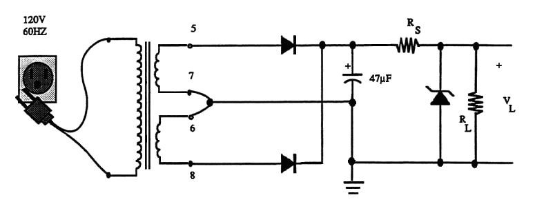 Fig. 8. Regulated DC power supply.
4.3 Disconnect RL and measure the voltage and current across the Zener diode.
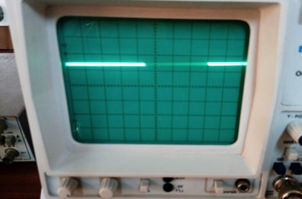 Fig. 9. Regulated DC output power supply.
Results and Discussions:
– In addition to the questions posted in the lab procedure, do and answer the following;
1. Plot the V-I characteristic the Zener diode.
2. What is the value of the forward resistance of the Zener diode?


